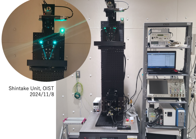
EUV Lithography project
EUV lithography based on our design can work with smaller EUV light sources, reducing costs and dramatically improving reliability and lifetime of the machines. It also consumes less than one-tenth the power of conventional EUV lithography machines, helping the semiconductor industry become more environmentally sustainable.
This technology has been made possible by solving two issues that were previously considered insurmountable in this field. The first involves a novel optical projection system consisting of only two mirrors. The second involves a new method to efficiently direct EUV light onto logic patterns on a flat mirror (the photomask) without blocking the optical path.
For more details, please see the OIST press release dated July 29, 2024.
Please refer to the following paper for the results of the optical system simulation:
Can we improve the energy efficiency of EUV lithography?arXiv:2405.11717
(Links to an external site)


