05 January 2015
OIST Patents New Nanoparticle Method
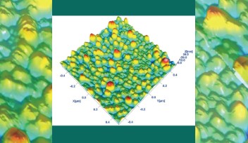
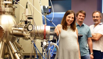
The Nanoparticles by Design Unit at the Okinawa Institute of Science and Technology Graduate University is constantly finding new ways to endow the tiniest of particles with more specific properties. They have developed methods to control the size and chemical composition of nanoparticles, and now they have found a way to control the degree of crystallinity, or the way that atoms align inside the nanoparticles. A nanoparticle’s crystallinity impacts its optical, magnetic, and electrical properties. Professor Mukhles Sowwan and the researchers in his unit Dr. Cathal Cassidy and Vidyadhar Singh have applied for a patent for their method, which describes exactly how to create semiconductor nanoparticles of varying crystallinity.
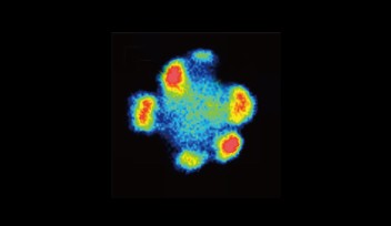
“Most scientists and even companies nowadays are using nanoparticles not optimized for their applications or devices,” explains Sowwan. “We hope, at a certain time, we will optimize the nanoparticles for specific applications.” To start though, the researchers in the Nanoparticles by Design Unit must figure out how to control a few basic characteristics of nanoparticles, such as crystallinity. A crystalline nanoparticle will have all of its atoms aligned in neat rows, while an amorphous nanoparticle will have more disordered atoms. A polycrystalline structure has atoms aligned in groups, which are also known as grains. Crystallinity is responsible for profound differences between products made of the same material. For example, soot is amorphous carbon, or carbon without any crystal grains, while diamonds are crystalline carbon.
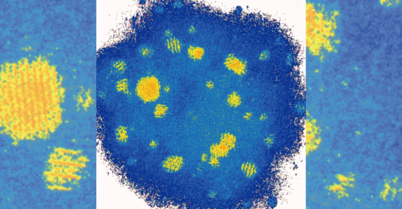
“It’s the first time to control the crystallinity and the number of crystallites of very small semiconductor nanoparticle,” Sowwan says, explaining that people have long known how to induce crystallinity in bulk semiconductor materials. But part of the reason why Sowwan can control certain characteristics is because of the experimental method he and his researchers use, based on a modified nanoparticle deposition system. One of the most important features of this system is the possibility to interact with or modify freshly formed semiconductor nanoparticles in flight before reaching a substrate. “That substrate is problematic,” explains Sowwan, “because it is always impacting the properties of the nanoparticle.” Following the steps described in the newly suggested method, nanoscientists expose these nanoparticles in flight to a beam of metal atoms. The metal atoms diffuse onto the surface of the nanoparticles and form metal nanoclusters, just a few nanometers wide, inducing crystallization in the product. The researchers can then selectively remove the metal nanoclusters with plasma cleaning, a fairly simple physical procedure, retaining only the intact semiconductor nanoparticles of desired crystallinity.
The new patent will credit this method to OIST. “To use this method for commercial purposes, such as engineered nanoparticles in solar cells or for medical bio-imaging, the technology will have to be licensed from OIST,and academic researchers will have to credit us in their research.” Sowwan says this is one of many characteristics he would like to control in order to produce more specialized nanoparticles. At the end of the day, this is one new set of directions in the rulebook of how to customize a nanoparticle.
For more information -- Patent application number: WO 2014141662 A1, Metal Induced Crystallization of Semiconductor Quantum Dots
Specialties
Submit a press inquiry


